Printing a Future
By Scott Michael Slone
You hear it humming and whirring, probably right next to you. It’s a small device that somehow takes your words and images and makes physical copies of them, all day long, and never stopping. It’s obviously your printer, but there’s a device coming around that would fit that description just the same, and yet has a much grander use. At the moment it exists as massive and expensive facilities, or centers and companies devoted to its use. It’s called nanofabrication, and researchers at Northwestern University are making it happen.
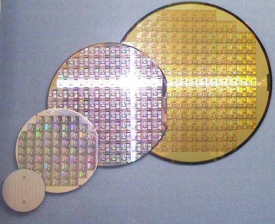
Nanofabrication is the set of techniques for building structures and devices at extremely small scales. It differs from 3D printing, where hardening ink is used, and instead uses light beams to either carve or build structures. Top-down nanofabrication methods, which carve away material from the structure, are already fairly common. You’re using one of their creations right now! The circuitry in your computer is created this way, and an example of the silicon wafers used can be seen on the left. Top-down’s reversed sibling is bottom-up nanofabrication. Imaginative titles right? Bottom-up, instead of removing material, adds it in layers until a 3-dimensional structure is completed. Bottom-up has numerous uses in the realms of electronics and molecular devices, but isn’t as commonplace as Top-down. Nanofabrication facilities, called foundries, are extremely expensive, getting upwards of several billion dollars to build and maintain. If nanofabrication is going to become commonplace, this excessive cost needs to be reduced, and researchers at Northwestern University are doing their part.
What the researchers have created involves numerous microscopic pyramids, all arranged in a grid. At the tip of each pyramid is a small aperture of only 100 nanometers in width. A light beam is then fired and separated into thousands of smaller streams, using the same process found in a projector. The light streams go into the pyramids at their bases, and fire out from the tips. The light beams interact with the surface of the material and react, modifying it and producing structures. The process is simple to explain, but is a careful synchronization of numerous processes at once. The result, however, is a rapidly produced nanostructure that only took a few hours to produce, in a device about the same size as an office printer.
The researchers, headed by Chad A. Mirkin, professor of Northwestern’s Weinberg College of Arts and Sciences, are quickly working on commercializing this product. The materials needed to produce the tool are easily available, and Mirkin expects the device could appear on the market in as little as two years. This device, equally capable of both Top-down and Bottom-up nanofabrication, could help make prototyping of such devices much more commonplace. Who knows? It may have other uses, and twenty years from now, in the occasional engineering firm, there may be a large object sitting next to the printer. It will be working hard, and printing the future.
Scott Michael Slone is C2ST’s resident intern. He is currently a senior at Illinois institute of Technology, majoring in Materials Science and Engineering. He enjoys the work C2ST is doing to help promote science and technology in the Chicagoland region, and is glad to help them as well. His scientific interests include nanotechnology and molecular machines. He hopes you’ll enjoy his technical tidbits on these and other subjects.
Works Cited
White, E. (2013, July 19). Desktop Printing at the Nano Level. Retrieved from Northwestern University: http://www.northwestern.edu/newscenter/stories/2013/07/desktop-printing-at-the-nano-level.html
Silicon Wafer Image care of Wikipedia.